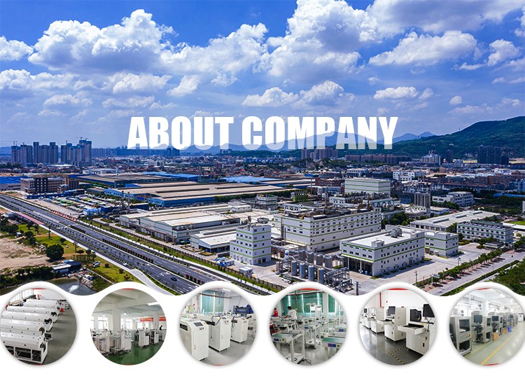
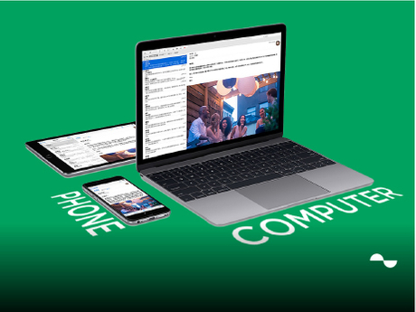
Computers and Phones
Computers and mobile phones are the most common electronic products in our daily life. They all adopt modern electronic technology and communication technology, providing great convenience and entertainment for people.
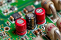
Computers are composed of central processing units, memory, hard disk, graphics card, motherboard, power supply, etc., used for computing, storage, processing and display of various information.
The mobile phone is a portable communication terminal, composed of processor, memory, screen, camera, battery and so on.
SMT technology is one of the most commonly used production technologies in the electronic manufacturing industry, widely used in the production of mobile phone and computer PCB boards.
For PCB boards, SMT technology can realize high-precision automatic mounting of electronic components and fast reflow welding, effectively improving production efficiency and quality. At the same time, SMT technology can also achieve miniaturization and lightweight circuit boards, making mobile phones and computers more portable and easy to use.
The production and manufacturing of these products are inseparable from SMT and DIP production processes.
SMT ( Surface Mount Technology) and DIP ( Dual in-line Package) are two different processes used in PCB assembly of computers and mobile phones.
The SMT process is primarily used to mount surface-mounted components, such as microchips, capacitors, resistors, and inductors, directly onto the PCB’s surface. This method is highly automated, utilizing precision chip mounters to place components with exceptional accuracy, often within ±30μm. SMT is ideal for compact, high-density PCB designs, which are common in smartphones and laptops, where space optimization is critical. The process supports the integration of advanced components like System-on-Chip (SoC) modules and miniaturized sensors, enabling devices to deliver high performance in slim form factors. Additionally, SMT enhances signal integrity and reduces parasitic capacitance, which is crucial for high-speed processors and memory modules in computers and 5G-enabled mobile devices.
In contrast, the DIP process focuses on through-hole components, such as sockets, switches, and connectors, which are inserted into pre-drilled holes on the PCB and soldered in place. DIP is valued for its mechanical robustness, making it suitable for components that endure frequent physical interaction, like USB ports or power switches on computers. While less automated than SMT, DIP ensures durability in applications where components must withstand stress, such as in rugged laptops or mobile devices designed for harsh environments. The process is also used for legacy components or specialized modules that require secure mounting to maintain long-term reliability.
Both SMT and DIP have distinct advantages and are selected based on the specific needs of the device. SMT excels in high-volume production and miniaturization, critical for modern smartphones with intricate multilayer PCBs. DIP, however, is preferred for components requiring strong physical anchoring, ensuring stability in devices like desktop PCs with modular expansion slots. In many cases, a hybrid approach combining SMT and DIP is employed to balance performance and durability. For instance, a smartphone’s PCB may use SMT for its processor and memory chips, while DIP secures its charging port. To enhance device performance, manufacturers incorporate specialized materials like EMI Shielding Foam in select assemblies.
This material, often placed discreetly within the PCB layout, mitigates electromagnetic interference, ensuring stable operation of sensitive components like antennas in mobile phones. The choice of SMT, DIP, or a combination thereof depends on factors like component type, device form factor, and production scale. By leveraging these processes strategically, manufacturers achieve the precision, efficiency, and reliability demanded by today’s computers and mobile phones, driving innovation in consumer electronics.
More details about Advanced Electronics PCB Assembly SMT Solutions for Computers and Phones, please Contact Us for freely.
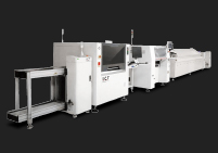
Following are the Solution for your reference.
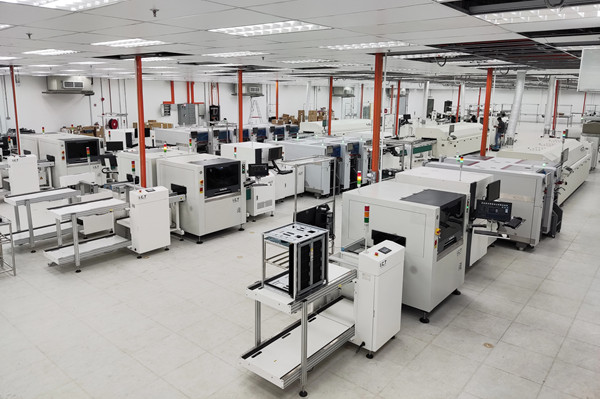
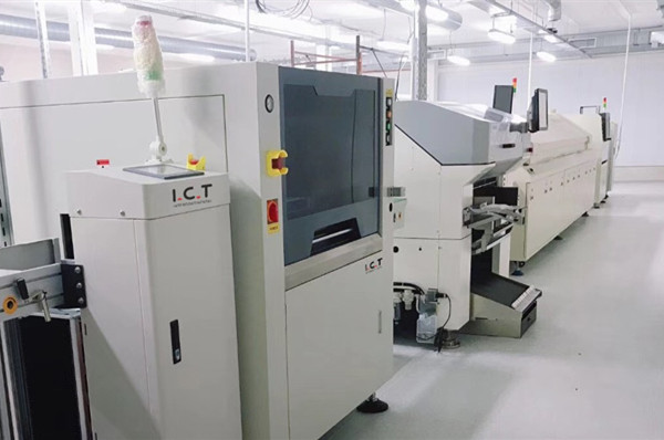
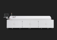
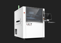
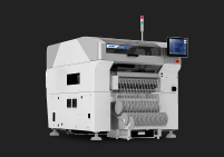
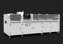
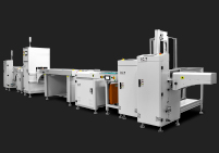
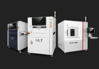
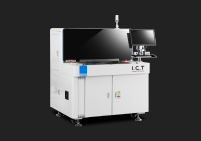
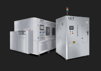
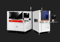
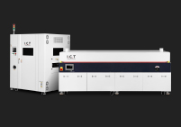
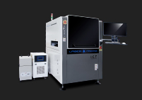
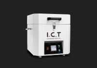
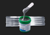
SMT Process: Solder Paste Printing --> SPI Inspection --> Components Mounting --> AOI Optical Inspection --> Reflow Soldering --> AOI Optical Inspection --> X-ray Inspection
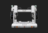
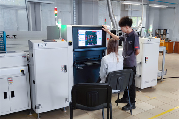
Advanced Electronics PCB Assembly SMT Full-line Solution equipment as follows: : 1 person to operate the whole line, 1 person to assist, total 2 people.

 English