English
Views: 0 Author: Site Editor Publish Time: 2024-08-23 Origin: Site


Surface Mount Technology (SMT) is a method used in electronics manufacturing where components are directly mounted onto the surface of printed circuit boards (PCBs). SMT has become the standard manufacturing process in the electronics industry due to its efficiency, cost-effectiveness, and ability to produce compact, high-performance electronic devices. In this article, we will explore the SMT manufacturing process in detail, including each step and related terms.
Before diving into the SMT manufacturing process, it's important to understand some key terms:
PCB (Printed Circuit Board): A board used in electronics to mechanically support and electrically connect electronic components.
SMD (Surface-Mount Device): Components that are designed to be mounted directly onto the surface of PCBs.
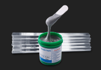
Solder Paste: A mixture of powdered solder and flux used to attach SMDs to PCBs.
Reflow Soldering: A process where solder paste is heated to its melting point to create permanent electrical and mechanical connections between components and the PCB.
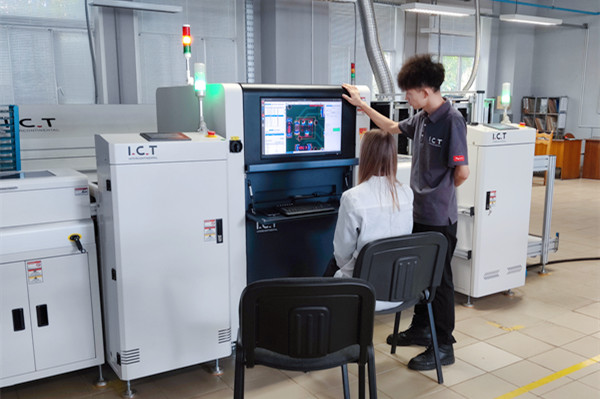
AOI (Automated Optical Inspection): A machine-based visual inspection process that uses cameras to detect defects in PCBs.
AXI (Automated X-ray Inspection): An inspection method using X-rays to check solder joints and connections hidden beneath components.
SPI (Solder Paste Inspection): The process of checking the quality of solder paste application on a PCB.
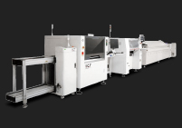
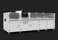
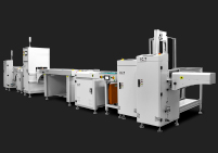
The SMT manufacturing process consists of several steps, each critical to ensuring the reliable placement and soldering of electronic components onto a PCB. Below is a detailed overview of each step in the SMT process.
The first step in the SMT manufacturing process is applying solder paste to the PCB. Solder paste is a sticky substance made from tiny solder balls mixed with flux. It is applied to the areas of the PCB where components will be mounted, typically onto metal pads.
Stencil Alignment: A metal stencil with cutouts corresponding to the solder pad locations on the PCB is placed over the board. The stencil acts as a mask to ensure that solder paste is only applied to the desired areas.
Paste Application: A squeegee or similar tool spreads the solder paste across the stencil, forcing it through the openings onto the PCB beneath. The thickness and uniformity of the paste layer are critical for ensuring proper component attachment and soldering.
Stencil Removal: The stencil is carefully lifted away, leaving precisely deposited solder paste on the PCB pads.
Proper solder paste application is crucial as it determines the quality of the solder joints and overall assembly reliability.
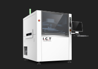
After applying the solder paste, the next step is Solder Paste Inspection (SPI). This step is vital to ensure that the solder paste is correctly deposited on the PCB.
Automated Inspection: SPI machines use cameras and sensors to scan the PCB and measure the volume, height, area, and position of the solder paste deposits.
Quality Control: The inspection data is analyzed to detect any defects, such as insufficient paste, excess paste, or misaligned deposits. These defects can lead to poor solder joints, component misplacement, or short circuits.
Feedback Loop: If defects are detected, adjustments can be made to the solder paste printer setup or process parameters to correct the issue. This feedback loop ensures high-quality solder paste application.
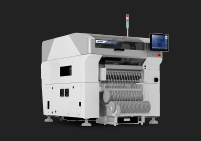
Once the solder paste has been inspected and verified, the next step is Chip Mounting, also known as component placement.
Component Preparation: SMT components, or SMDs, are supplied in reels, trays, or tubes and fed into the pick-and-place machine.
Pick-and-Place: The pick-and-place machine uses robotic arms equipped with vacuum nozzles to pick up components from the feeders and place them onto the solder-pasted pads on the PCB. The machine’s high precision ensures that components are accurately positioned according to the PCB design.
Alignment and Placement: The machine uses vision systems and alignment algorithms to ensure each component is placed correctly. The speed and accuracy of modern pick-and-place machines allow for high-throughput production.
Chip mounting is a critical step as any misalignment or misplacement can result in defective boards that require costly rework or scrapping.
After the automated placement of components, there is often a need for a Visual Inspection and the placement of some components by hand.
Visual Inspection: Skilled operators visually inspect the boards to check for misaligned components, missing parts, or any obvious defects that the machines may have missed. This step is often done using magnifying tools or microscopes.
Manual Component Placement: Some components, especially those that are non-standard, large, or sensitive, may need to be placed manually. This could include connectors, transformers, or odd-shaped components that automated machines cannot handle effectively.
Adjustments: If components are found to be out of place or missing, operators can manually adjust or add these components to ensure all parts are correctly positioned before soldering.
This step helps ensure that any errors from the automated process are caught early, reducing potential defects in the final product.
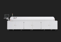
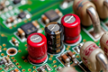
Once all components are in place, the PCB assembly moves on to Reflow Soldering, where the solder paste is melted to form permanent electrical and mechanical connections.
Preheat Zone: The PCB assembly is gradually heated in the reflow oven to remove any moisture and to bring the board and components to a temperature just below the solder’s melting point.
Soak Zone: The temperature is maintained to activate the flux in the solder paste, which cleans the metal surfaces and prepares them for soldering.
Reflow Zone: The temperature is rapidly increased to above the solder paste’s melting point, causing the solder balls to melt and form solder joints between the components and the PCB pads.
Cooling Zone: The assembly is slowly cooled to solidify the solder joints, ensuring a strong mechanical and electrical connection.
Reflow soldering is critical as it determines the quality of the solder joints, which affects the performance and reliability of the final electronic device.
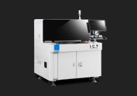
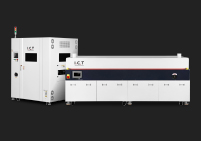
After reflow soldering, the assembly undergoes Automated Optical Inspection (AOI) to detect any defects in the placement or soldering of components.
High-Resolution Imaging: AOI machines use high-resolution cameras to capture detailed images of the PCB assembly from multiple angles.
Image Analysis: The machine compares the captured images against a known good reference, looking for deviations such as missing components, incorrect polarity, solder bridges, or tombstoning (where components stand on one end).
Defect Detection: The AOI system flags any defects for review. Boards with detected defects are either sent for rework or marked for further inspection.
AOI helps maintain high quality by ensuring that only defect-free boards proceed to the next stage of production.
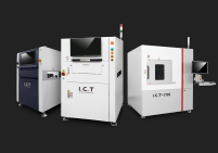
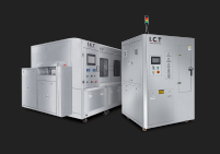
For components with hidden solder joints, such as Ball Grid Arrays (BGAs), an Automated X-ray Inspection (AXI) is required to inspect solder quality.
X-ray Imaging: AXI machines use X-rays to penetrate the PCB and create images of the solder joints hidden beneath components.
Defect Analysis: The X-ray images are analyzed to check for defects such as voids, solder bridges, or insufficient solder coverage, which are not visible through optical inspection.
Quality Assurance: Boards with defects are flagged for rework or scrapping, depending on the severity and rework feasibility.
AXI is essential for ensuring the reliability of components with hidden solder joints, as undetected defects can lead to device failure.
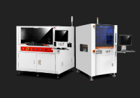
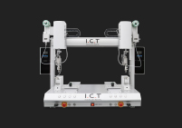
The final step in the SMT manufacturing process is In-Circuit Testing (ICT) or a Functional Test to ensure that the PCB assembly meets all electrical and functional specifications.
In-Circuit Testing (ICT): This test checks the individual components on the PCB, such as resistors, capacitors, and ICs, to ensure they are correctly placed and functioning. ICT also checks for shorts, opens, and correct solder connections.
Functional Testing: In this test, the PCB is powered up, and specific functions are tested to ensure that the board performs as expected. Functional testing simulates the actual operating conditions the PCB will face in its final application.
Defect Identification and Rework: If any defects are identified during ICT or functional testing, the board is sent back for rework. This may involve replacing components, re-soldering, or adjusting assembly settings.
ICT and functional testing are the last steps to ensure the quality and functionality of the final product, minimizing the risk of defective products reaching the customer.
The SMT manufacturing process involves several precise steps, from solder paste printing to final functional testing. Each step is crucial to ensuring the quality, reliability, and performance of the final electronic product. By understanding the details of each step in the SMT process, manufacturers can produce high-quality electronics that meet today’s demanding standards.